VLSI Cadence Design

(Jan. 2024 - April. 2024)
Introducing digital circuits building using Cadence.
Introduction
After learning more about digital circuits, I studied Cadence Layout to present and simulate digital circuits in a professional manner. Here, I will show designs of a Systolic Array, Full-Adder and a 4-bit Up/Down Counter.
Systolic Array
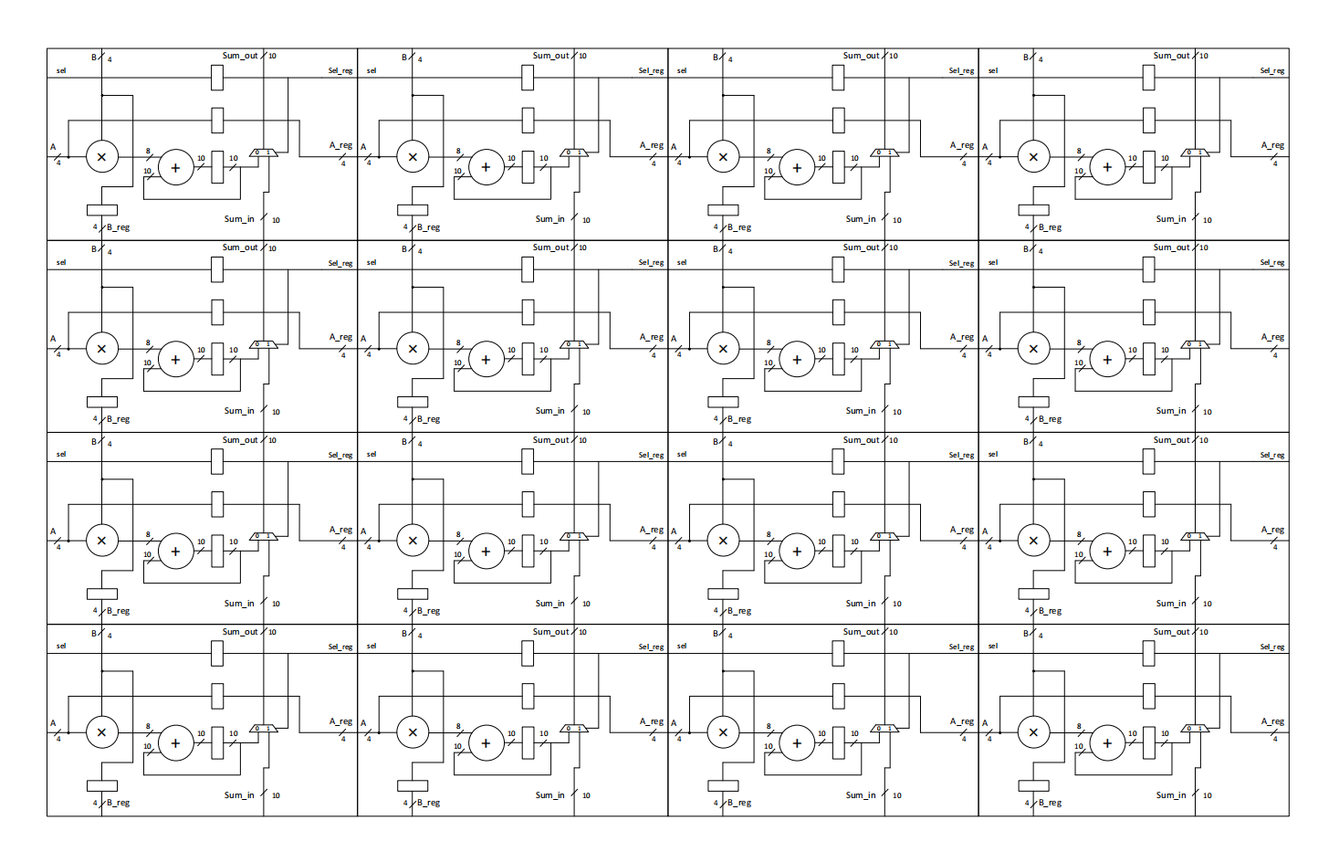
In this project, my group and I designed a full-custom 4x4 Systolic Array capable of performing matrix multiplication on two 4x4 matrices. The design utilizes interconnected processing elements, where each processing element consists of a multiplier and a carry-skip adder. Each carry-skip adder efficiently handles the accumulation process by reducing propagation delay, enhancing the overall performance of the array. The processing elements receive data inputs from neighboring elements in a pipelined fashion, ensuring efficient data flow and parallel computation. The array was constructed by systematically arranging these processing elements, with registers to synchronize data inputs and outputs across the system. Please refer to the screenshots for my detailed implementation and design.
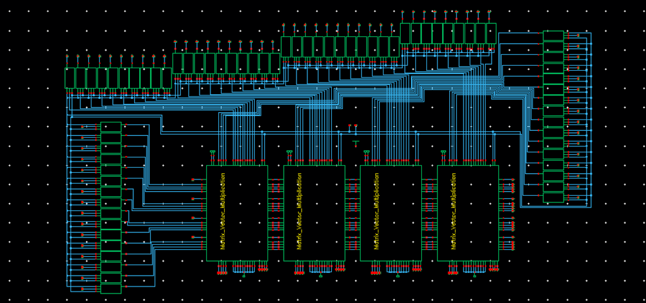
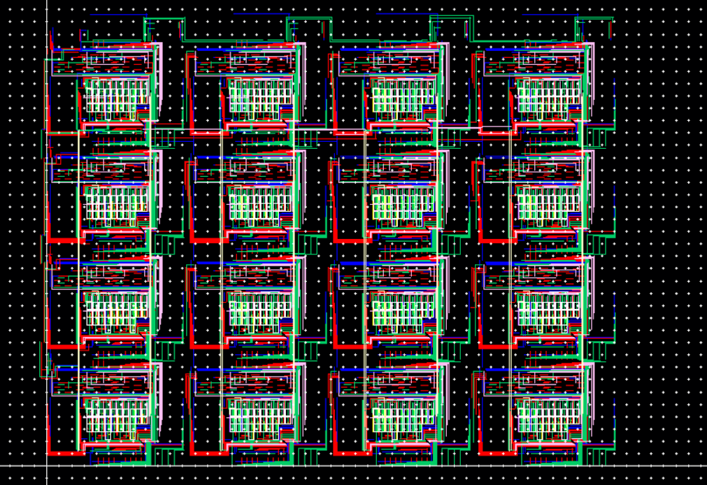
The performance of the design exceeded expectations, operating reliably at 200 MHz with a 5 ns clock period. Despite the relatively large area of 43.608 mm², the design demonstrated an excellent balance between functionality and efficiency. Considering it was a full-custom implementation, the outcome was highly satisfying, showcasing a robust and scalable solution for systolic array-based computations.
Full-Adder
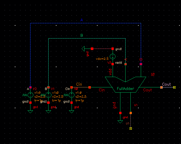
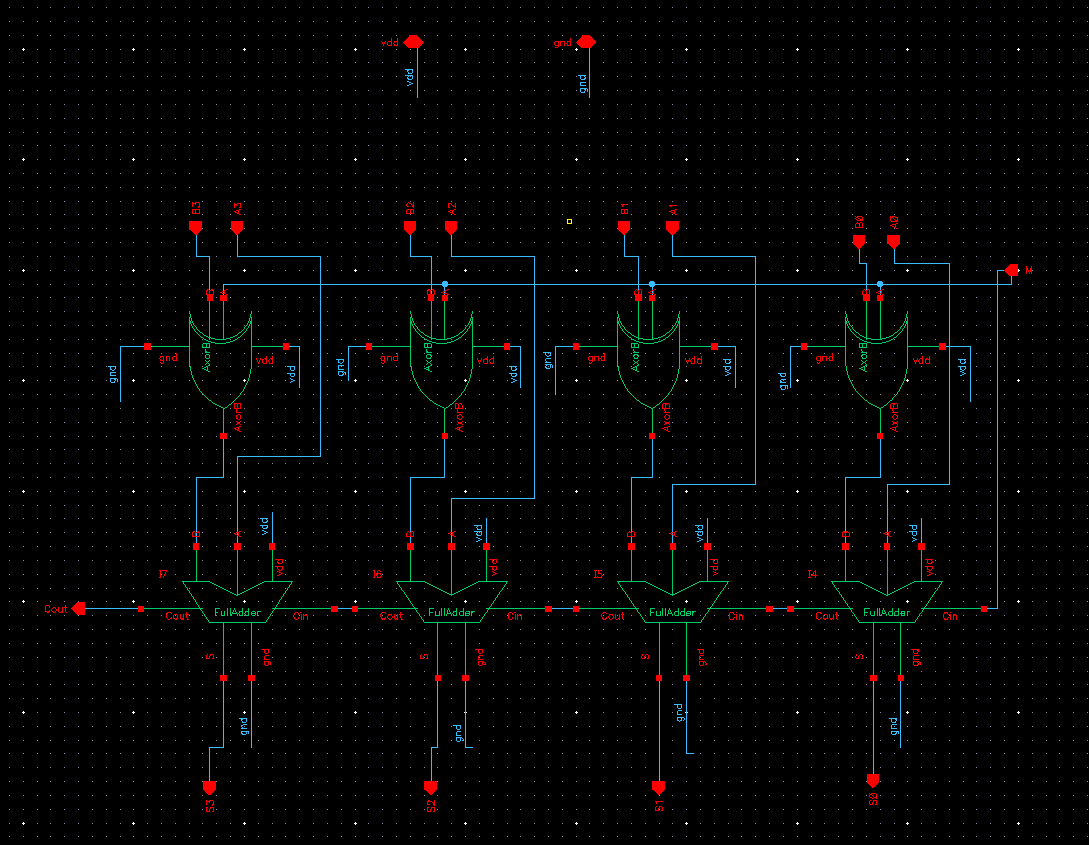
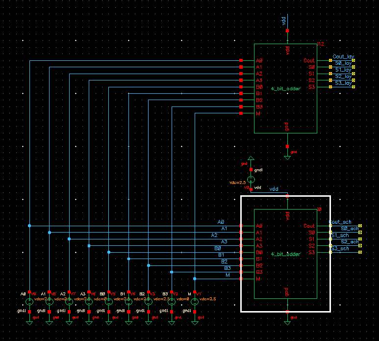
In this project, I designed a 4-bit full adder and subtractor circuit capable of adding or subtracting two 4-bit input numbers, denoted as A = A3A2A1A0 and B = B3B2B1B0. The process began with creating a 1-bit full adder using NAND and XOR logic gates. By connecting four 1-bit full adders and incorporating XOR gates at the inputs, I constructed the 4-bit full adder.

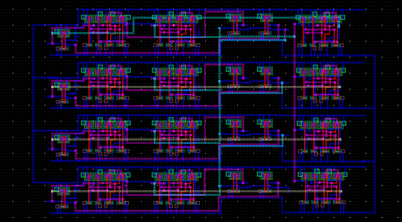
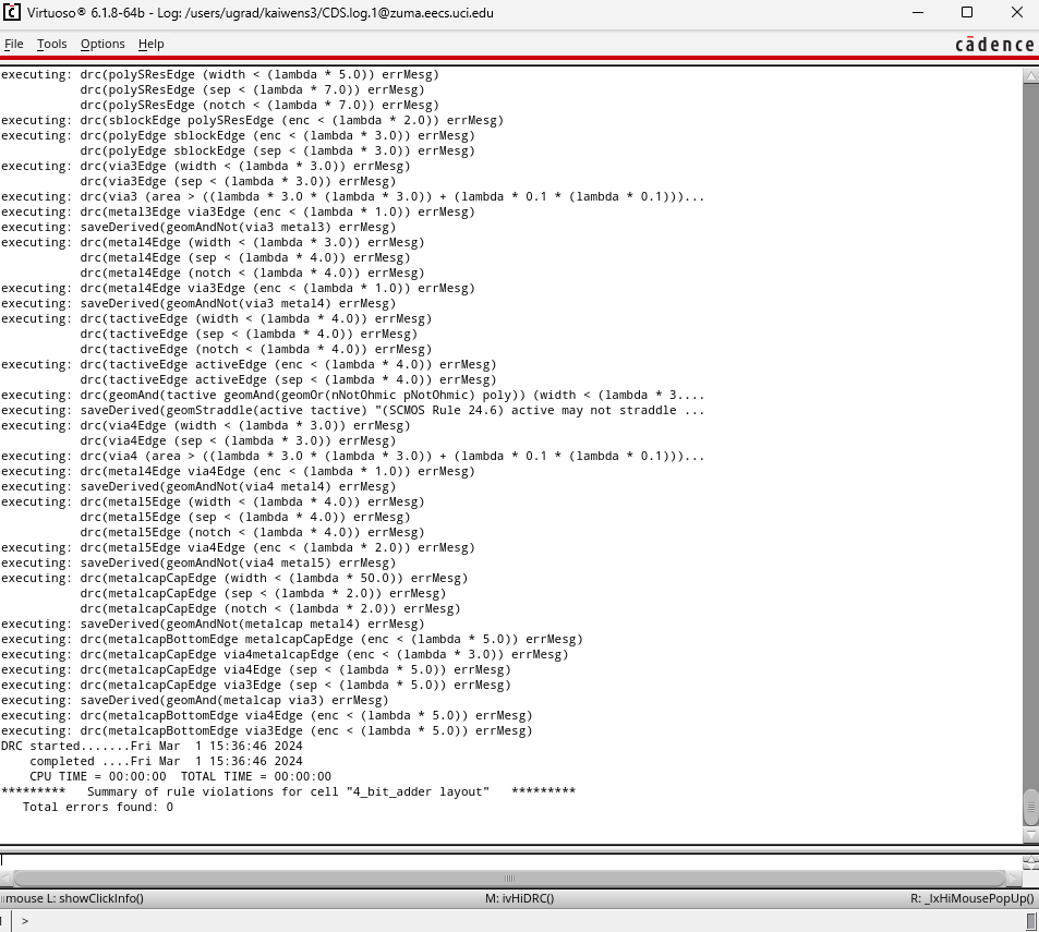
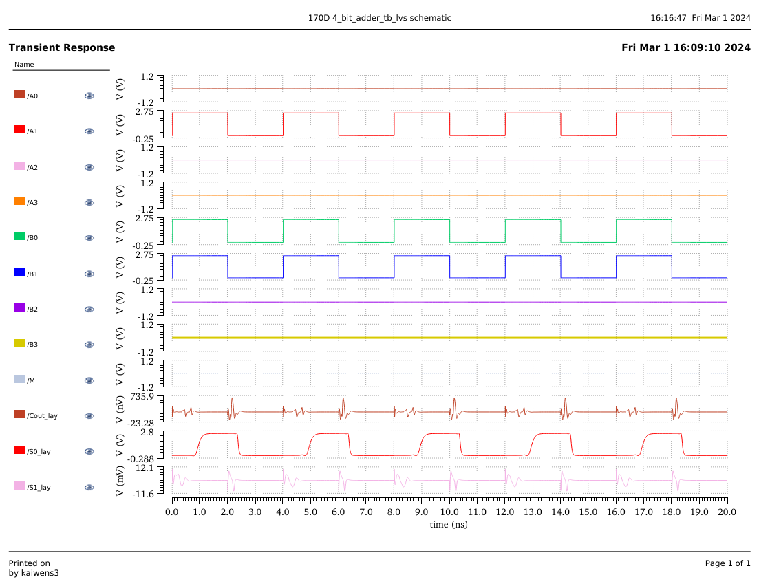
To facilitate the subtraction operation, a logical 1 is sent to the control bit input (K) of the adder. This signal is directed to Cin1 of the first adder and the XOR gates that process each bit of B. For addition, the control bit input (K) is set to logical 0. After developing the schematic for the full adder, I proceeded to create the layout and compared the outputs of the schematic and the post-layout schematic to ensure accuracy and functionality. The following are the building blocks of the 4-bit Full Adder.
Inverter Design
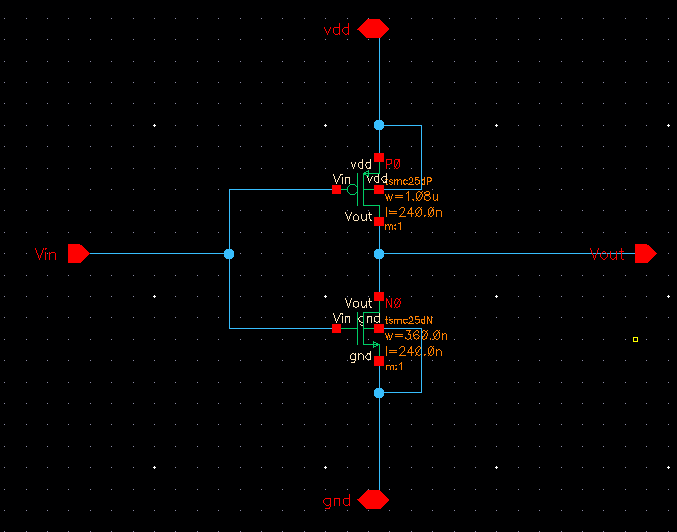
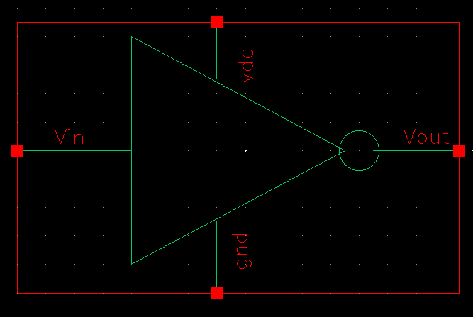
1. Inverter Schematic. 2. Inverter Symbol.
NAND Gate Design
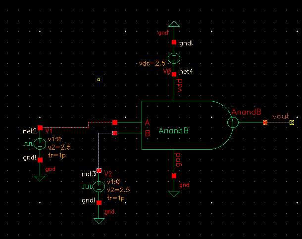
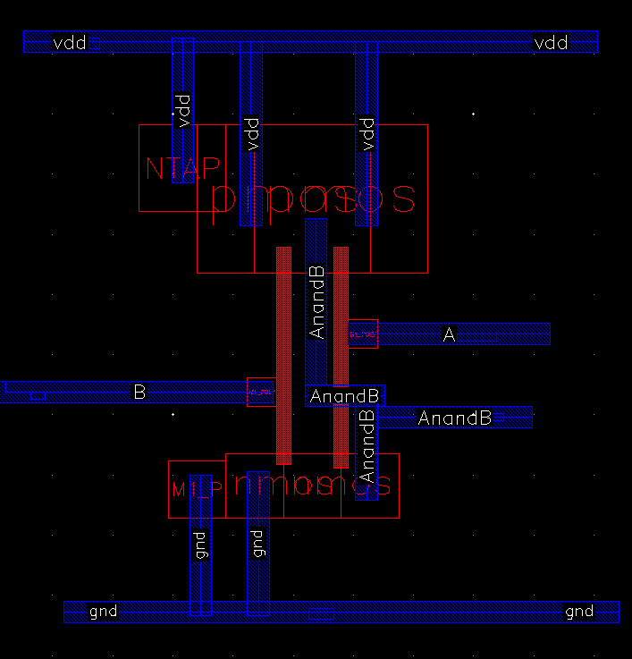
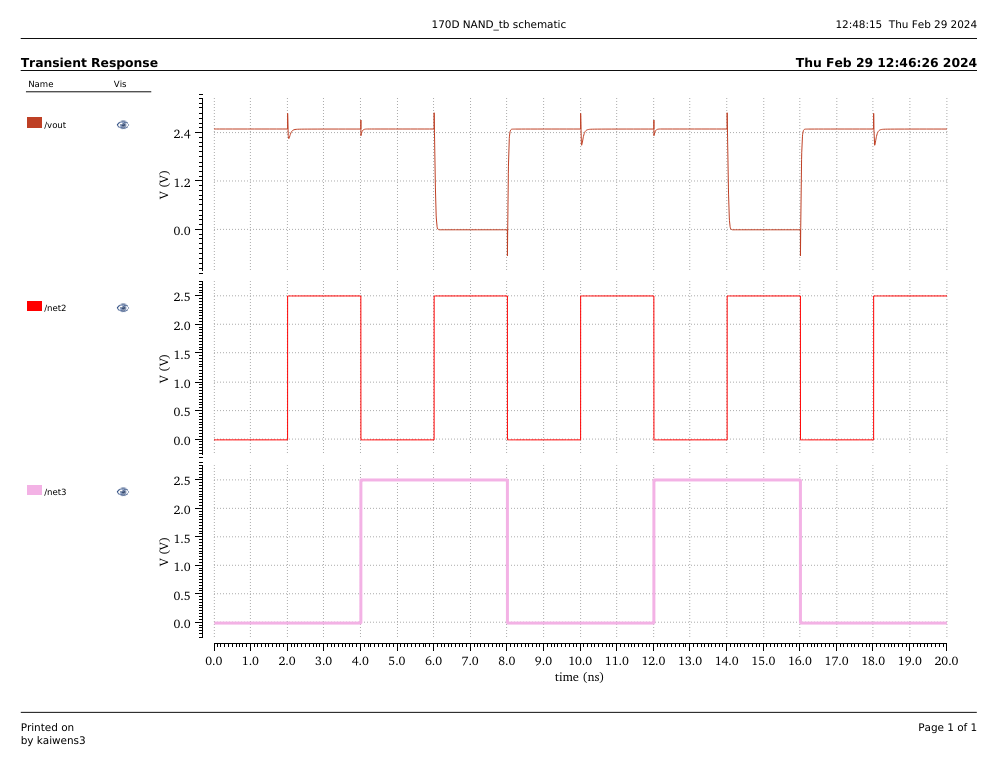
1. NAND Gate Symbol. 2. NAND Gate Layout. 3. NAND Gate Simulation
XOR Gate Design
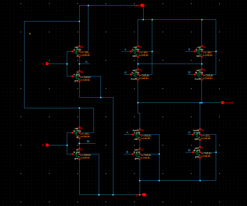
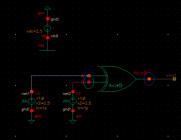
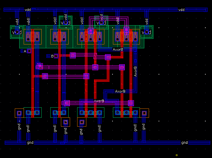
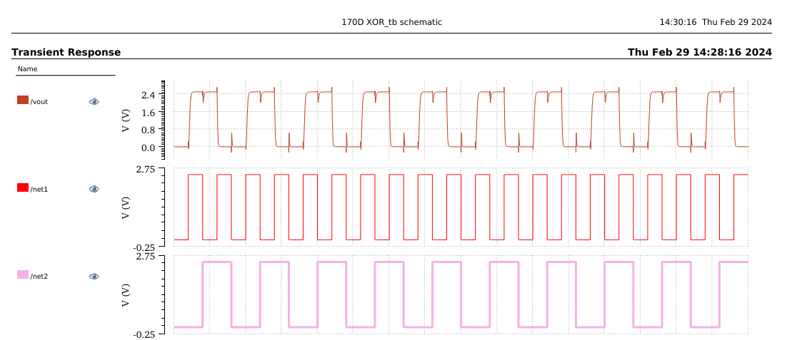
1. XOR Gate Schematic. 2. XOR Gate Symbol. 3. XOR Gate Symbol. 4. XOR Gate Simulation
1-Bit Adder Design

4-Bit Full Adder Design
4-bit Up/Down Counter
In this project, the objective is to design a 4-bit binary up/down counter. The design process begins with the creation of a master-slave JK flip-flop, utilizing two D latches built from NAND gates. By combining four of these JK flip-flops with additional logic gates, the counter is designed to output 4 bits (Q0-Q3), representing the number of clock cycles. The project involves simulating both the schematic and post-layout schematic of the counter, and analyzing the output waveforms in response to varying inputs.
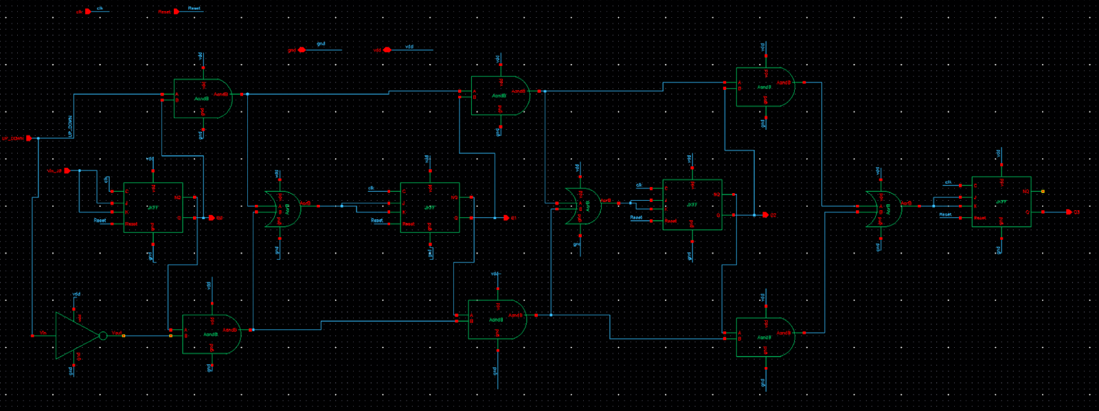
In theory, the 4-bit up/down counter will increment or decrement with each clock pulse. The counter is designed to represent numbers from 0 to 15 (0000 to 1111 in binary) when counting up, and from 15 to 0 when counting down. The counter has four inputs: reset, up_down, Vin for J0 & K0, and clock. The reset input must be set high for the counter to operate. The up_down input determines the counting direction—high for counting up and low for counting down. Vin for J0 and K0 should remain high, typically connected to Vdd, to ensure proper operation. The clock input is crucial, as the counter's response is based on the clock’s period and pulse width. The design utilizes JK flip-flops because they toggle states on the rising edge of the clock. With both J and K inputs connected to logical 1 (Vdd), the flip-flops alternate their output with each rising clock edge, enabling the counter’s counting function.
The following are the building blocks of the 4-Bit Counter.
JK Flip-Flop
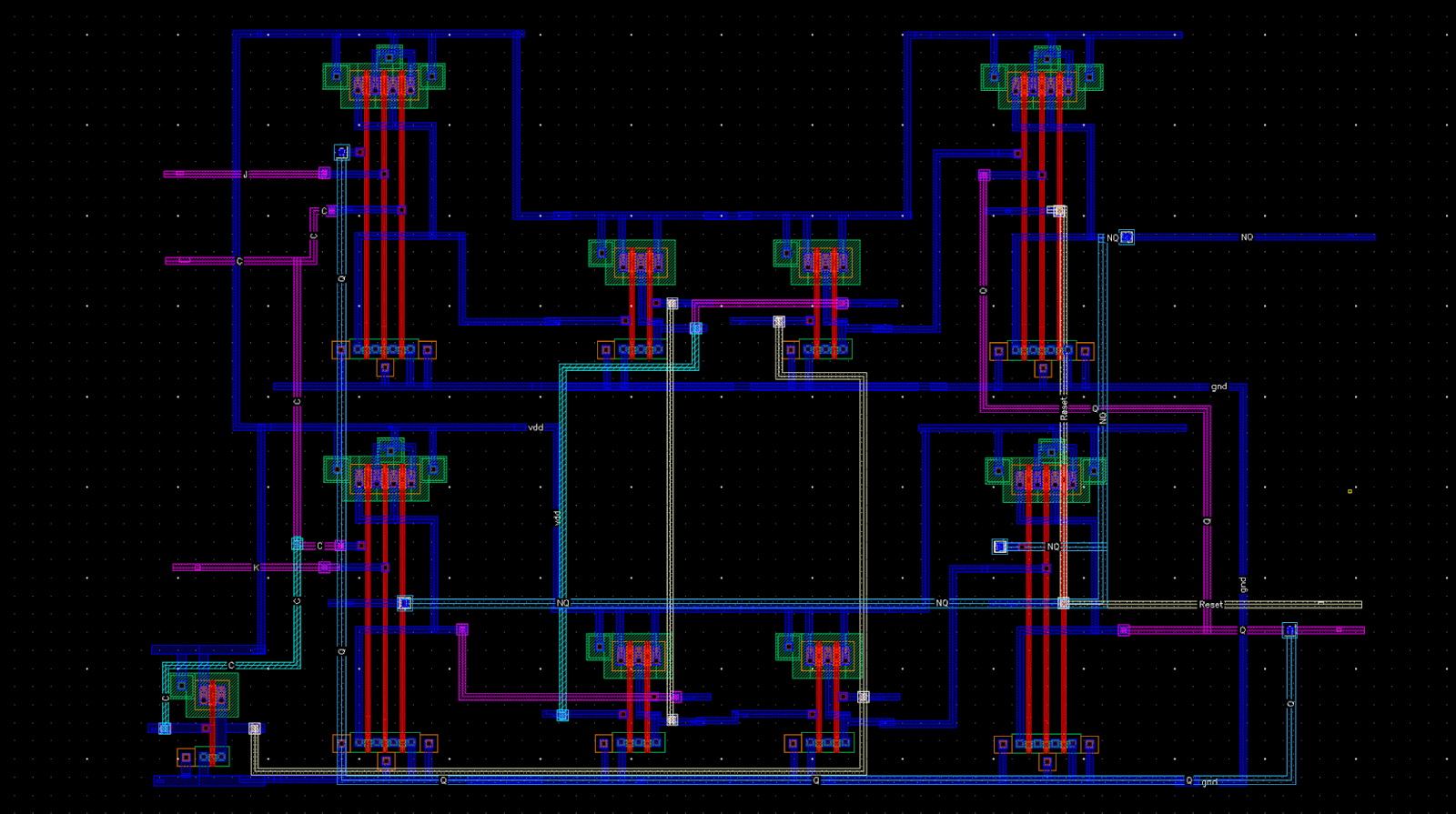
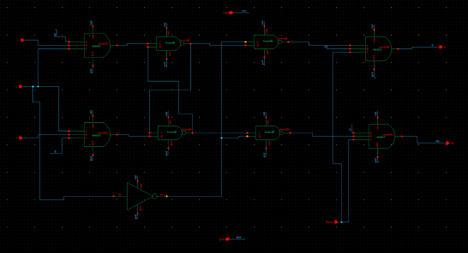
JKFF Layout and Schematic

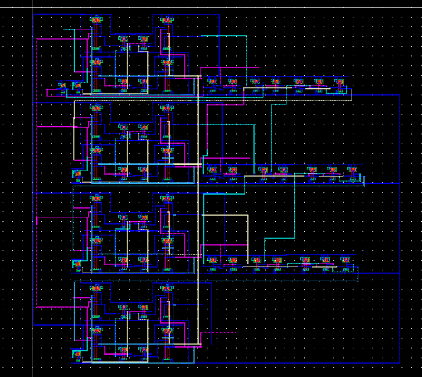
4-Bit Up/Down Counter Schematic and Layout
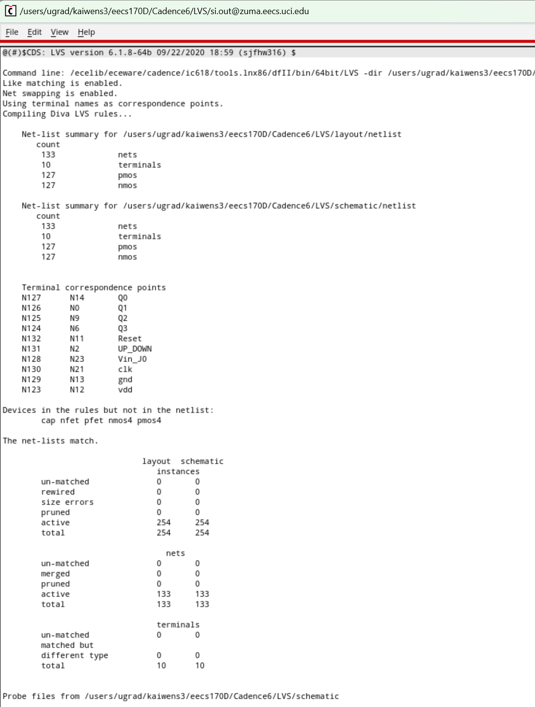
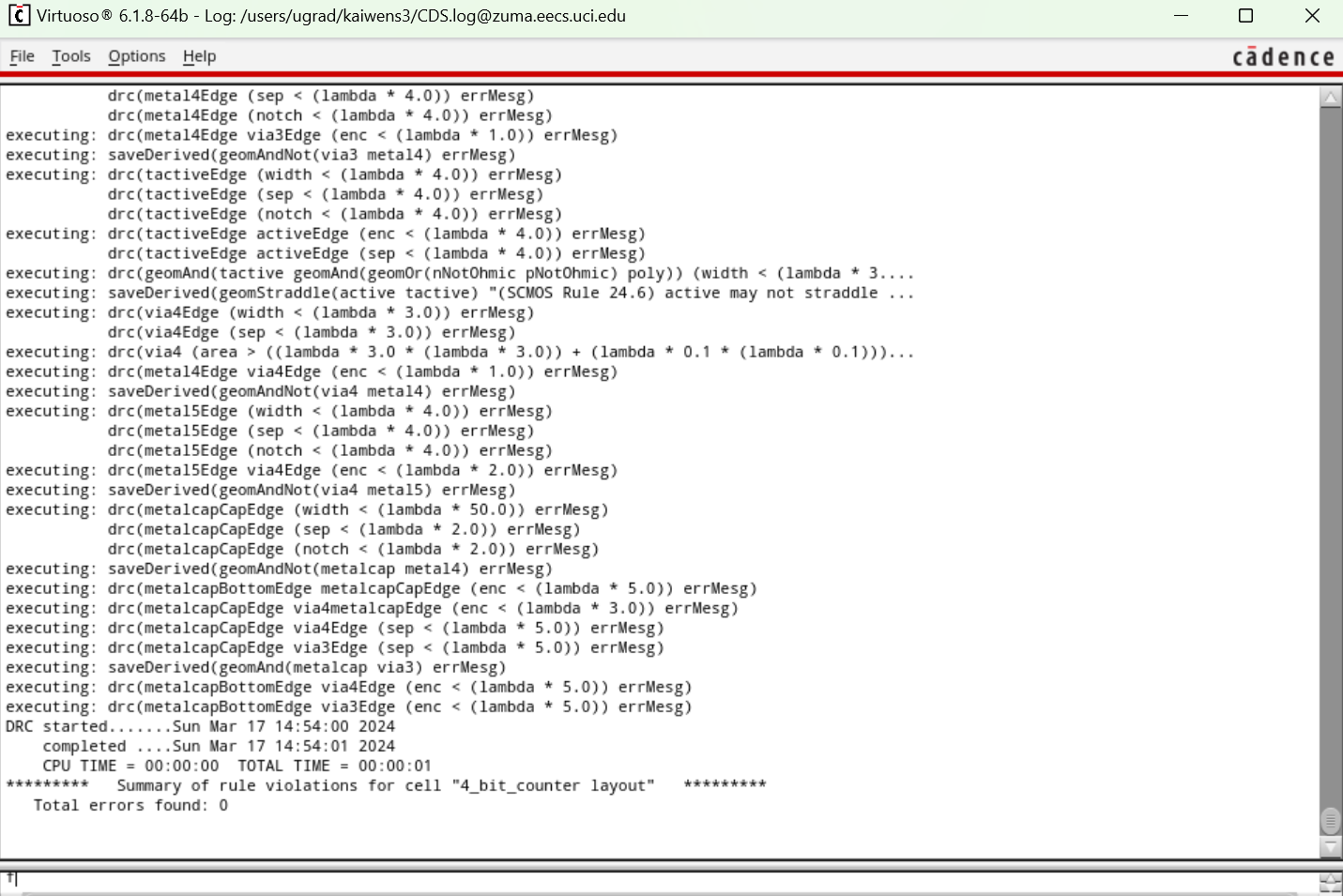
4-Bit Up/Down Counter DRC & LVS
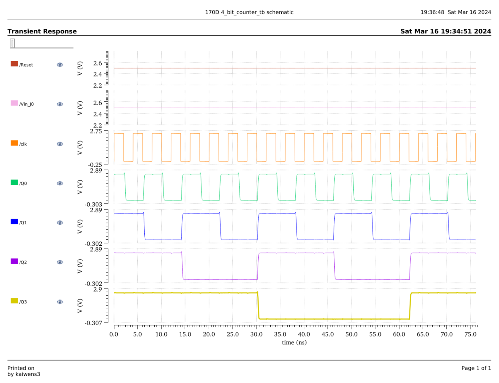
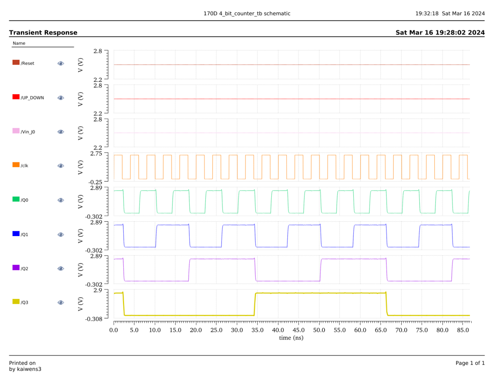
Counting Up & Down Simulation
Special Thanks
Kiril Afonchenko – – Teammate – – kafonche@uci.edu